NVDLA analyze
1. Overview
The overall structure of the NVDLA is shown in the following figure.
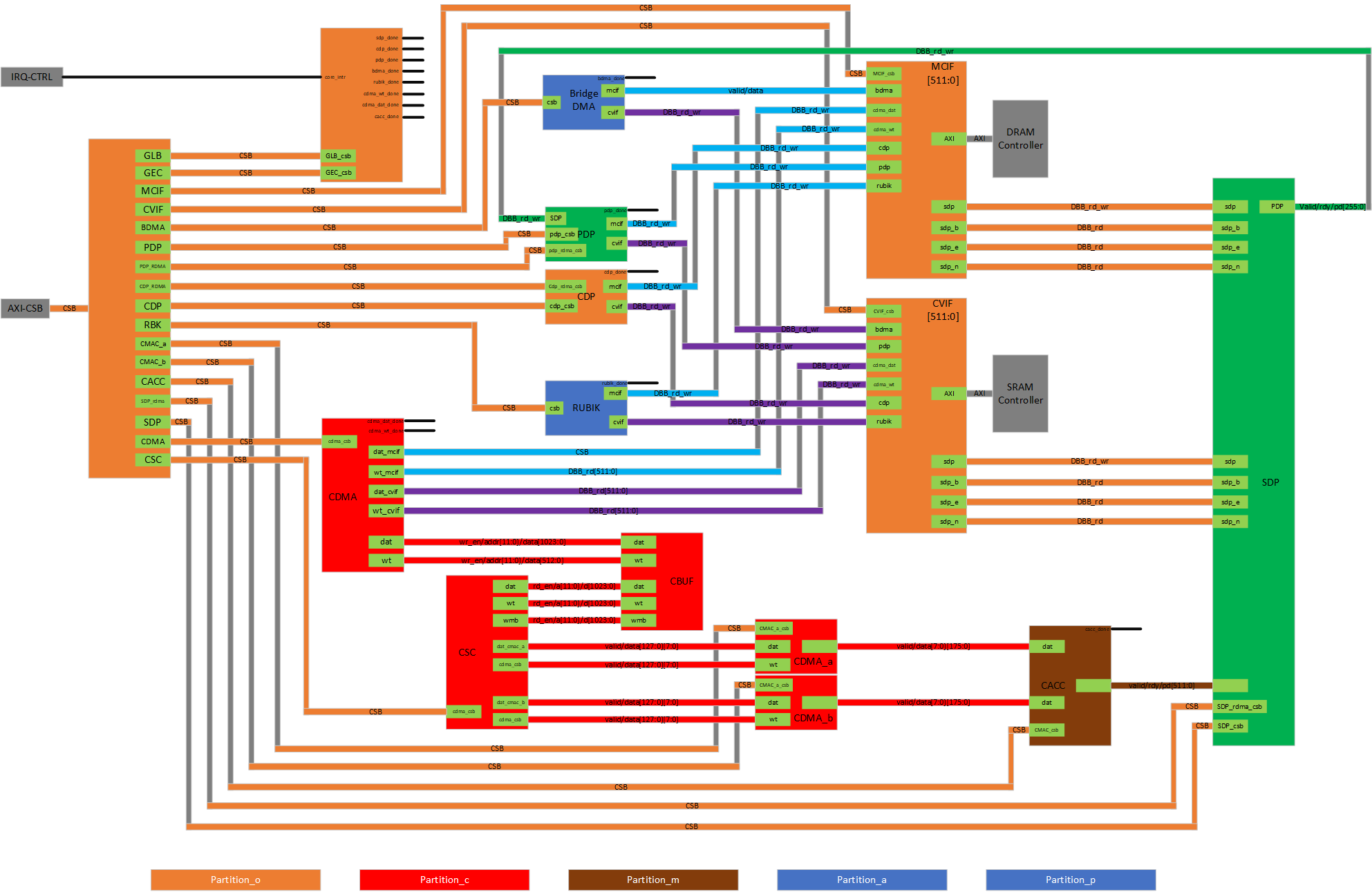
It can be divided into five sections.
|-- TOP_MODULE.v
    |-- NV_NVDLA_patition_o.v
    |-- NV_NVDLA_patition_c.v
    |-- NV_NVDLA_patition_m.v
    |-- NV_NVDLA_patition_a.v
    |-- NV_NVDLA_patition_p.v
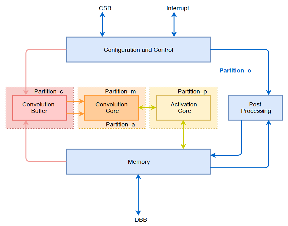
Partition_ocontrols the communication between processing elements with external controllers and memory units.Partition_cmanages various convolution kernel operations such as CDMA, CBUF, and CSC.Partition_mperforms multiplication and addition computations. This Convolution MAC module comprises of 16 MAC cells. Each of these cells includes 64 16-bit multipliers and 72 adders.Partition_aaccumulates the partial sums from the MAC arrays and estimates the results before sending it to the next stage of activations.Partition_pperforms various linear and non-linear operations as discussed.
2. Memories
2.1. RAMDP(Dual-Port SRAM)
2.1.1. Interface
This section describes a dual-port SRAM design. The macro is designed to perform read and write operations independently.
| Pin | Type | Presence | Description |
|---|---|---|---|
CLK_R |
Input;Clock | Default | Memory read clock |
CLK_W |
Input;Clock | Default | Memory write clock |
READ_[msb:0] |
Input | Default | Synchronous read address input |
RD_[msb:0] |
Output | Default | Memory read data output |
RE |
Input | Default | Synchronous read enable |
WADR_[msb:0] |
Input | Default | Synchronous write address input |
WD_[msb:0] |
Input | Default | Synchronous write data input |
WE |
Input | Default | Synchronous write enable |
Misc. Pins. These will depend on the target RAM library for whether they’re necessary.
| Pin | Type | Presence | Description |
|---|---|---|---|
IDDQ |
Input | Default | Asynchronous stand-by mode enable pin |
SLEEP_EN_[7:0] |
Input | Default | Power gating controls |
RET_EN |
Input | Default | Retention enable |
RET_SVOP[1:0] |
Input | Default | Timing margin control pins |
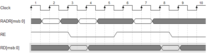
2.1.2. Read timing
Next graph describes the reading timing of the dual-port RAM:
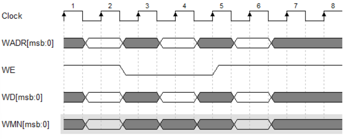
2.1.3. Write timing
Next graph describes the writing timing of the dual-port RAM:
2.2. RAMPDP: Pseudo-Dual Port SRAM
This section describes an embedded pseudo-dual port SRAM macro. The RAMPDP macro behaves like a dual port RAM, but is created by double clocking a single port RAM.
2.2.1. Interface
The following enumerates the RAMPDP pins and corresponding functions.
| Pin | Type | Presence | Description |
|---|---|---|---|
CLK |
Input;Clock | Default | Memory clock |
READ_[msb:0] |
Input | Default | Synchronous read address input |
RD_[msb:0] |
Output | Default | Memory read data output |
RE |
Input | Default | Synchronous read enable |
WADR_[msb:0] |
Input | Default | Synchronous write address input |
WD_[msb:0] |
Input | Default | Synchronous write data input |
WE |
Input | Default | Synchronous write enable |
Misc. Pins. These will depend on the target RAM library for whether they are necessary.
| Pin | Type | Presence | Description |
|---|---|---|---|
IDDQ |
Input | Default | Asynchronous stand-by mode enable pin |
SLEEP_EN_[7:0] |
Input | Default | Power gating controls |
RET_EN |
Input | Default | Retention enable |
RET_SVOP[1:0] |
Input | Default | Timing margin control pins |
2.2.2. Timing
Next graph describes the timing of the Pseudo Dual Port RAM:

3. In-memory data formats
4. Partition_o
This partition controls the communication between processing elements with external controllers and memory units.
4.1. Overview
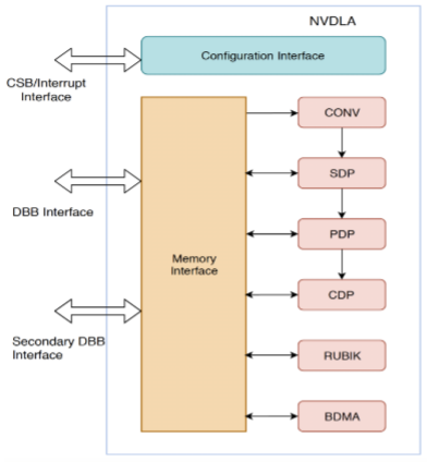
CSB - This module reads and writes configuration registers of each
layer in NVDLA core. This transfers data from the external manage-
ment processor through the APB interface.CFGROM - This maintains configurable parameters of the core for its
respective specification definition.MCIF - This interface communicates with all subunits that access the external DDR. This data bus uses an AXI protocol.
PDP and CDP - These units perform pooling and local response nor-
malization respectively.GLB - They control the output interrupt signals of all the sub cores of NVDLA.
As shown in the blue part of the figure below.
4.2. CSB
The CSB bus consists of three channels : the request channel , the read data channel , and the write response channel. The channels are as described below.
4.2.1. Clock and reset
The CSB interface uses a signal clock domain , shared between NVDLA and the requester.
4.2.2. Request channel
The request channel follows a valid/ready protocol; a data transaction occurs on the request channel when and only when the valid signal (from the host) and the ready signal (from NVDLA) are both asserted in the same clock cycle. Each request to CSB has a fixed request size of 32 bits of data, and has a fixed 16bit address size. CSB does not support any form of burst requests; each packet sent down the request channel is independent from any other packet.
| Data field | Bits | Direction | Description |
|---|---|---|---|
csb2nvdla_valid |
1 | Input | Indicates that a request is valid |
csb2nvlda_ready |
1 | Output | Indicates that the receiver is ready to take a request |
csb2nvlda_addr |
16 | Input | Address.Aligned to word boundary |
csb2nvdla_wdat |
32 | Input | Write data |
csb2nvdla_write |
1 | Input | Write flag.1'b0:Request is a read request.1'b1:Request is a write request |
csb2nvlda_nposted |
1 | Input | Non-posted write transaction indicator.1'b0: Request is a posted write request.1'b1: Indicates a non-posted write request.Posted write transactions are writes where the requester does not expect to and will not receive a write completion from receiver on write ack channel. The requester will not know if the write encounters an error. Non-posted write transactions are writes where the requester expects to receive a write completion or write error on write ack channel from receiver. |
4.2.3. Read data channel
The read data response channel is described in the below table. NVDLA returns read-response data to the host in strict request order; that is to say, each request packet (above) for which “write” is set to 0 will have exactly one response, and that response cannot jump forward or backwards relative to other reads.
The read data channel follows a valid-only protocol; as such, the host cannot apply back-pressure to the NVDLA on this interface.
| Data field | Bits | Direction | Description |
|---|---|---|---|
nvdla2csb_valid |
1 | Output | Indicates that read data is valid |
nvdla2csb_data |
32 | Output | Data corresponding to a read request , or zero in the event of an error |
4.2.4. Write response channel
The signals associated with the write response channel are described in the below table. NVDLA will return write completion to the host in request order for every non-posted write.
The write completion channel also follows a valid-only protocol, and as such, the host cannot back-pressure NVDLA on this interface.
| Data field | Bits | Direction | Description |
|---|---|---|---|
nvdla2csb_wr_complete |
1 | Output | Indicates that a CSB write has complete |
4.2.5. Inference timing
Following picture shows the timing of CSB interface.
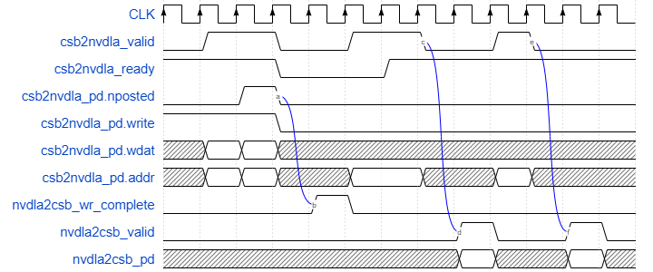
第一个时钟为posted的写模式,在读入csb2nvdla_valid和csb2nvdla_ready均为高电平时读入data和addr,并写入,不返回信号。第二个为non-posted写模式,在nposted电平为高时读入此时的数据和地址,并将ready信号置为低电平,写入完成后返回一个写完成信号(nvdla2csb_wr_complete置为高电平)随后将csb2nvdla_ready信号返回高电平。第三个为读信号,如图所示,当ready信号为低电平时不读入任何数据,当ready信号为高电平时读入此时的读地址,读取到数据后,返回一个读数据有效信号(nvdla2csb_valid),并返回读数据。第四次与第三次大体相同。
The firset clock is ‘posted’ write mode, when csb2nvdla_valid and csb2nvdla_ready are both high, read data and addr, and write. The second is non-posted write mode, when nposted is high, read data and addr, and set ready to low. After write complete, return a write complete signal(nvdla2csb_wr_complete is high), and then return csb2nvdla_ready to high. The third is read mode, as shown in the figure, when ready is low, no data is read. When ready is high, read the read address at this time, and return a read data valid signal(nvdla2csb_valid) after reading the data. The fourth and third are basically the same.
4.3. CFGROM
4.4. MCIF
4.5. PDP
4.6. CDP
4.7. GLB
5. Partition_c
6. Partition_m
7. Partition_a
8. Partition_p
Reference
- [1] NVDLA